Yes you heard me right we are braking out of the box! We will be doing some soldering and making our own PCF8591 breakout board.
In this example we are going to connect to PCF8591 AD/DA Converter without using a pre-made breakout board.

When connecting to PCF8591 AD/DA Converter in the previous example then we used a breakout board that had the PCF8591 chip, and some support components.
The issue with going this way is that the breakout board had no way to set the base address for the i2c bus which limits us to one such board which is total of 4 analog inputs and 1 analog output. But what if we needed 2 analog outputs ? Or 6 analog inputs ? This is why we will be making the breakout board by our self’s in this example so that we can set address for the i2c bus and connect 2 boards on the bus. Which will enable us to connect up to 8 such boards, getting possibility of up to 32 analog inputs and 8 analog outputs.
Another for building our own is to limit power usage. I skip totally debug LED on the analog output. And debug power on LED I put a jumper on it so it can be disabled to save power.
Disclaimer:
We do not take any responsibility for possible errors in the guide or errors that you might do wiring it up. Incorrect wiring can result in damaged sensor or damaged Raspberry PI.
Pieces we use in this example:
- Raspberry PI 2 (or Raspberry PI 3 or maybe Orange PI which are also great for GPIO)
- Cobbler and Cobbler cable
- WiringPI needs to be installed on the Raspberry PI -> See here.
- I2CTools needs to be installed on the Raspberry PI and I2C needs to be enabled in the Raspberry PI settings.
- 5x 10kΩ resistors.
- 2x 0.1 µF ceramic capacitors (or one 0.2 µF)
- PCF8591 chip (just the chip not brake-out board) (Those usually come surface mounted, but if you shop around you can probably also find them suitable for breadboard, I took surface mounted to get best price and I was planning to solder anyhow, in this example I will be making one of them usable for breadboard though for initial testing). Those do cost a bit, I paid around $9 with free shipping to Iceland for 20 surface mounted chips.
- Adaptor PCB board if the PCF8591 is surface mounted which is the most common for this chip.
- LED
- 1x 1kΩ resistor.
- Some header pins
- Jumper
- DIP switch (3 button. (Or you can use jumpers if you don’t want to get fancy)
Other things you almost definitely will need in this project:
- Soldering Wick ! — To fix errors, you will need it in this project if you are dealing with surface mounted chip.
- Soldering magnifier.
If you are not familiar with breadboards, how to place a cobbler on the breadboard or need to know how to read the color codings on the resistors then click here bellow
Using breadboard Resistor color codings
Wiring diagram for our custom made brake-out board:

Now the plan is to build it first on breadboard to test and fine tune for possible errors and then build it on a decent board that can be used as component. (This turned out to be good plan since there was error in the design that I caught in the breadboard test and fixed the design after figuring it out)
First issue with this plan was that it would call for making breadboard friendly PCF8591 adapter. And right here the project got stuck, first realisation was that I need adapter PCB since you will not solder such chip to normal test PCB, their way to small to fit on that. Then finally a PCB adapter came and then I realised I had taken wrong. Its tricky not only is it pin count but also width of the chip and density of the pins.

The one on the left was the correct one, but the one on the right had right density by was not wide enough.

You will probably always need magnifier when soldering this one no matter how good your vision is.
Once I finished soldering then it looked like this:

I made two of those, one for the Breadboard experiment and one for the final build.
Now I measured from each pin on the chip to each header pin to make sure everything was all right. It was good I did this testing at this point as one pin was not good on one of the boards so I had to fix.
The breadboard experiment:

(Sadly I could not find 3 way dip switch for the drawing program so the drawing shows 2x 2 way, but it should be 1x 3 way)
To test this then this is applied the same way as is shown in the pre-made board in the PCF8591 Analog To Digital guide. (Except you may want to download updated code at bottom of this guide that can set alternate hardware addresses depending on your DIP switch settings)
Once this was working perfectly reading the analog input channels and writing to the analog output channel then it was time to build the final board.
The final board:
I wanted the PCB adaptor for the chip to be like plug in that I could take out of the main board like as if it was breadboard. But sadly my header pins were rectangular and the female socket pins I had were circular. So I had to skip this niceness for now.
I started making it without having the PCP adaptor board in, this way I was able to fit some things under the chip and use the space there.

So this is how it was before installing the chip “daughter board”. Header pins, Resistors, LED, capacitors and the DIP switch are all in place.
Then at last I soldered the “daughter board” in as seen bellow.

As you can see then my board did not end up to be a lot bigger than the bought one. I don’t know why the bought ones do not expose the hardware address and instead put jumpers for useless on board Light sensor and Potentiometer. Its as if their made only for showcase and not for practical uses.
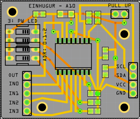
On the picture above the first DIP is set to one which will make the Hardware address 0x49 instead of 0x48.
The black pins on top right are Analog in 0 to 4 from top to bottom. The white pin on right is Analog out. Blue pin is GND, red pin is +5 V. Lower yellow pin (pin number 9 on the daughter board) is SDA, upper yellow pin is SCL (pin number 10 on the daughter board).
You can now use more than one of those on your SDA bus if setting one to different hardware address. This means you can even use the bought one and your own together since one may remain on address 0x48.
You can wire up to 8 in theory by using the dip switch addresses but of course you need to be aware of power management if having many devices.
If you are using more than one boards then do not use the cheap resistor way to convert the bus voltage but instead use a I2C logic converter as we both show how to build and how to use a pre-made one in our I2C logic level converter – Building our own guide. You only need one such converter as all the PCF8591 would plug on the 5V side and then the Raspberry on the 3V side. Like shown bellow:

After doing all this then I realised that I really should have jumper on the pull up resistors on the SDA bus. Only one device on the SDA bus should be using pull up resistors. Its often a problem that there is no way to disable them on brake-out board with out cutting out the resistors on one board if you have many SDA devices.
So after adding another jumper then schema looks like this:

Where if having more than one device on the SDA bus you pull out the JP2 given that the other device has pull up resistors in place.
Downloading the code:
After doing this all then I went ahead and did draw up PCB board ready to be fabricated. You many think this is expensive but it is not. I found service that will do 10 boards for $10, given you would else need to buy adapter for the chip and also base plate to solder on then the $1 per board is probably not bad deal !!
The board came like this from fabrication:

The following red marked areas are 10k resistors (SMD 0805 form factor):

The following red marked area is 1k resistor (SMD 0805 form factor):

The following are 0.1µF capacitors (SMB 0805 form factor);

And the red mark on this one shows the orientation of the main chip:

And finally a LED (SMD 1206 form factor). Greed shows the cathode of the LED.

And the final build:

Dip switches 1 – 3 set the hardware address.
Dip switch 4, turns on or off the power status light (to save power then you may want it turned off).
The Jumper at top left turns off the pull up resistors. Only one device on the bus should be using pull up resistors.
Note that soldering this one was not easy ! I used hot air touch free soldering, but still found it to be very hard.
Gerber files to fabricate copy the Einhugur A10 board
The boards were fabricated at AllPCB, if you use the link bellow to sign up there then both you and Einhugur should get discount. (Which of course would help support our effort here). Making your own boards is cheaper than you might think, for 10 boards we paid $10, so $1 per fabricated board, which is about same as just the chip adapter board costed in our first prototype.
That is it for now, by all means leave comments if you like this article or have questions.
 AliExpress.com Product – HoldPeak HP-770D Multimeter

